Playground · research instrument
DSP · AudioMicrostrip Impedance Calculator
Hammerstad-Jensen microstrip impedance solved live, propagation delay, S-parameters, eye diagrams that bite when mismatch grows. Animated voltage waves, magnetic vectors, Smith Chart, and FM hiss audio modulated by |Γ|.
Independent research instrument — not claimed as MakerPortal shipped product code. Methods, equations, assumptions, and limitations are disclosed so you can inspect what the page does and does not establish.
Trace Geometry
Termination & Frequency
Animated TEM wave + H-field vectors
Smith Chart — S11 live
Frequency sweep S11/S21
Red S11 mag, blue S21 mag dB vs 0.1-6GHz. White dot = current freq.
The math and physics, in full
Hammerstad-Jensen Z0
ε_eff with ΔW correction for finite copper thickness.
Reflection
Delay
Gear behind this build
Signal Integrity stack · 4 picks
Hardware picks4
 $72.88Book
High Speed Digital Design: A Handbook of Black Magic (Prentice Hall Modern Semiconductor Design)
Defines Hammerstad-Jensen Z0, skin depth delta=sqrt(2/ωμσ), and crosstalk K_b backward coupling — closed-form behind this lab's per-unit-length L,C extraction and NEXT/FEXT formulas.
 $12.69Diagnostic
HiLetgo USB Logic Analyzer Device with EMI Ferrite Ring USB Cable 24MHz 8CH 24MHz 8 Channel UART IIC SPI Debug
Budget 8-ch USB logic analyzer (sigrok/PulseView). Useful for RTOS GPIO timing and SI digital demos — not a Saleae substitute in bandwidth.
 $85.49Diagnostic
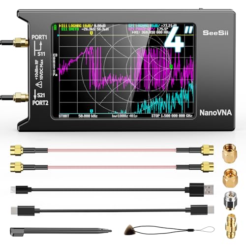
SEESII Upgraded NanoVNA-H4 Vector Network Analyzer, Latest V4.4 9KHz-1.5GHz HF VHF UHF 4" Touch Screen VNA Antenna Analyzer Measures S Parameters,Voltage Standing Wave Ratio, Phase,Delay, Smith Chart
Handheld VNA with touchscreen + SOL kit — S11/S21 lab companion for RF Bench and Antenna Sandbox.
 $13.90Kit
AURSINC SMA Calibration Kit and SMA Male to Male Jumper for NanoVNA H H4 F V2 V3 SAA Mini1300 PS100 Vector Network Analyzer Antenna Analyzer
SOL cal standards + SMA jumper for NanoVNA H/H4 — SI Lab and RF Bench SOLT demos.
Prices shown were retrieved from the Amazon Product Advertising API on 8 October 2026 and are indicative only — the price and availability on Amazon at the time of purchase apply.
More gear across every app: the full Gear list →
Hardware Kit Builder
Build the physical hardware platform. Select your components below to generate a live, real-time bill of materials and build instructions.
Build this lab
SI / S-parameter starter
NanoVNA + SMA SOL cal kit + Johnson’s Black Magic — measure what the microstrip model predicts.
- $85
- $14
- $73
- $13
Prices shown were retrieved from the Amazon Product Advertising API on 8 October 2026 and are indicative only — the price and availability on Amazon at the time of purchase apply.
Estimated total
$172
Prices from Amazon catalog cache · may change
Core solver
// src/lib/circuit-engine.ts — the module this page actually calls.
// Hammerstad & Jensen, "Accurate Models for Microstrip Computer-Aided Design",
// IEEE MTT-S Digest, June 1980. One model end to end: no piecewise u<=1 kernel,
// and no W/h <= 1/(2*pi) thickness branch (that split is Schneider 1969).
const ETA0 = 376.730313668;                      // CODATA 2018 sqrt(mu0/eps0)

function duThickness(u, th, Er) {                // th = t/h, BOTH normalised to h
  if (!(th > 0)) return 0;
  const k = Math.tanh(Math.sqrt(6.517 * u));
  const du1 = (th / Math.PI) * Math.log(1 + (4 * Math.E / th) * k * k);
  return 0.5 * du1 * (1 + 1 / Math.cosh(Math.sqrt(Er - 1)));   // Er = 1 -> factor 1
}
function z0Homogeneous(u) {                      // air-filled impedance, ohm
  const fu = 6 + (2 * Math.PI - 6) * Math.exp(-Math.pow(30.666 / u, 0.7528));
  return (ETA0 / (2 * Math.PI)) * Math.log(fu / u + Math.sqrt(1 + (2 / u) * (2 / u)));
}
function epsEffHammerstad(u, Er) {
  const a = 1 + Math.log((Math.pow(u, 4) + Math.pow(u / 52, 2)) / (Math.pow(u, 4) + 0.432)) / 49
              + Math.log(1 + Math.pow(u / 18.1, 3)) / 18.7;
  const b = 0.564 * Math.pow((Er - 0.9) / (Er + 3), 0.053);
  return (Er + 1) / 2 + ((Er - 1) / 2) * Math.pow(1 + 10 / u, -a * b);
}
function microstripZ0(W, H, Tmm, Er) {
  const u = W / H, th = Tmm / H;
  const u1 = u + duThickness(u, th, 1);          // air-filled corrected width
  const ur = u + duThickness(u, th, Er);         // dielectric-loaded corrected width
  const e0 = epsEffHammerstad(ur, Er), zr = z0Homogeneous(ur);
  const ratio = z0Homogeneous(u1) / zr;          // Tmm = 0 -> ratio = 1
  return { Z0: zr / Math.sqrt(e0), eff: e0 * ratio * ratio };
}
function gamma(ZL, Z0) { return (ZL - Z0) / (ZL + Z0); }Export · Soft gate
Export stackup + estimated S11/S21 sweep (CSV)
Tuned W/H/Er/T/L, Hammerstad-Jensen Z₀/ε_eff and an estimated S11/S21 sweep from 0.1 to 5.9 GHz as CSV — not a Touchstone .s2p file — free with watermark footer, clean after email unlock. Feed to PCBWay Shared Project for 10% fab credit path.
File · stackup-sweep.csv
stackup-sweep.csvtext/csv+ watermark line on free pathFree download adds a small footer:
# Export from makerportal.ai — free watermarked build. Unlock c…Clean export removes footer. Both are generated fresh from your current sim tuning.
Privacy: email stays in your browser localStorage (mp_export_email_signal-integrity-lab) + unlock flag (mp_export_unlock_signal-integrity-lab). If Buttondown username is configured, we also POST to Buttondown (privacy-first mode, no tracking pixels per D-014). See privacy → affiliates & email.
Unlock clean export
Soft gate — no hard paywall, no Clerk. Email stays local unless you explicitly check the newsletter box. Unsubscribe anytime. RSS at /rss.xml.
✓ Lab Pro — clean export on every lab
Your licence unlocks this and every other gated simulator, so there is nothing to enter here. Manage or sign out on the shop page.
✓ Unlocked — clean exports enabled
Stored in mp_export_unlock_signal-integrity-lab. Clean file omits watermark. Re-lock via browser devtools → localStorage.
Fabricate this design
From sim → PCB
Export your tuned stackup / Gerbers and order boards — supports shared-project revenue (10% PCB + 10% SMT) when you use our project link.
What you get
- Stackup CSV / Gerbers tuned in sim (W/H/εr, microstrip Z₀, array spacing → fab notes)
- PCBWay Shared Project if available — 10% PCB + 10% SMT revenue when others order same design
- Privacy-safe — no extra tracking beyond merchant checkout; disclosure in /privacy#affiliates
signal-integrity-labNo export yet — tune then exportOrder boards
Order on PCBWayReferral · 5%+↗PCBWay Shared Projects pay 10% PCB + 10% SMT — one fab conversion beats many Amazon electronics clicks.
Frequently asked questions
How is Z0 calculated?
Hammerstad & Jensen 1980, end to end. Finite copper thickness first WIDENS the strip: Δu = ½·(t/h)/π·ln(1 + 4e·tanh²(√(6.517·W/h))/(t/h))·(1 + sech(√(εr−1))), evaluated twice — at εr=1 for the air width u₁, at the real εr for the dielectric width u_r. Then Z0_air(u) = (η₀/2π)·ln(f(u)/u + √(1+(2/u)²)) with f(u) = 6 + (2π−6)·e^(−(30.666/u)^0.7528), ε_eff(u) = (εr+1)/2 + (εr−1)/2·(1+10/u)^(−ab), a = 1 + ln((u⁴+(u/52)²)/(u⁴+0.432))/49 + ln(1+(u/18.1)³)/18.7, b = 0.564·((εr−0.9)/(εr+3))^0.053. Z0 = Z0_air(u_r)/√ε_eff(u_r), and the reported ε_eff is scaled by (Z0_air(u₁)/Z0_air(u_r))². Thicker copper LOWERS Z0. There is no W/h ≤ 1/(2π) thickness branch and no piecewise u ≤ 1 impedance branch — both belong to older models (Schneider 1969, Hammerstad 1975).
What causes eye closure?
Two terms: reflection from Γ=(ZL-Z0)/(ZL+Z0) creating ISI via 2*Td delayed superposed pulse, and crosstalk NEXT ≈ (1/4)*(Cm/C+Lm/L)*Td/t_rise. Our eye generator convolves PRBS with Gaussian channel plus reflection echo amplitude Γ·exp(-αl). Mismatch >0.3 collapses eye height ~40% – heard as FM hiss increase.
Why Smith Chart matters?
Normalized z=Z/Z0 maps to Γ plane via Γ=(z-1)/(z+1). A microstrip line rotates Γ by θ=2βl: Γ_in=Γ_L e^{-j2βl}. Sweeping frequency traces a spiral. The chart in this lab updates S11 live as you drag W,H or stub. Center = 50Ω match.
How accurate is the solver?
TEM assumption ignores dispersion: ε_eff(f)=ε_eff(0)+dispersion correction Kirschning-Jansen valid to ~20 GHz for h=0.2mm. Loss α_c≈Rs/Z0*~geometry, α_d≈27.3*εr/(εr-1)*(ε_eff-1)/ε_eff * tanδ * f/c. Good to ±5% up to 6GHz; beyond need full-wave FDTD.
Shareable still
The instrument, captured—not illustrated.
This 16:9 frame is rendered from the real browser instrument above. It is the page's canonical preview for image search, link unfurls, and posts that need to show what the tool actually does.
Download 1280 × 720 JPEG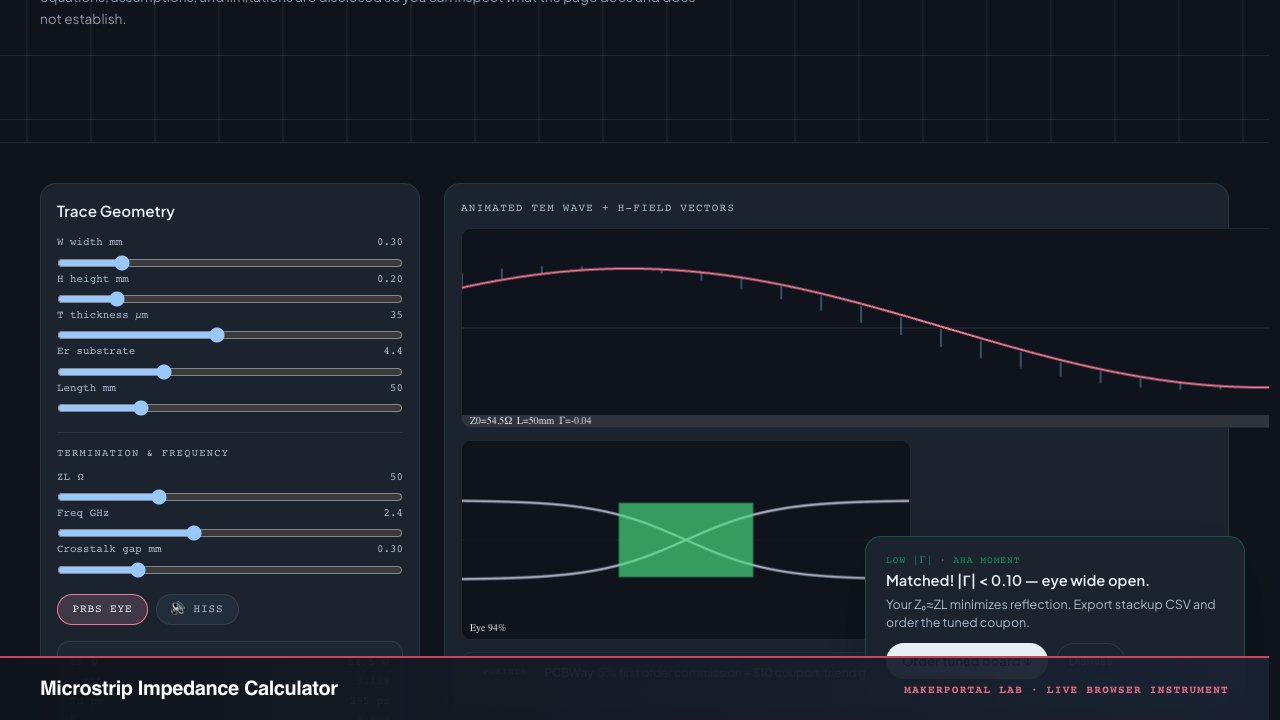
Continue the experiment
Related instruments
Edge DB Sync Lab
Place replicas on a world map, watch reads beat writes
Client vs Serverless GPU Benchmarker
Your GPU vs a cloud GPU, measured — never estimated
RF & Microwave Circuit Bench
S-parameters live on a Smith Chart, hum to pure tone at 50Ω